Samsung Reportedly Plans Texas AI-Memory Plant for AMD and Nvidia by 2030
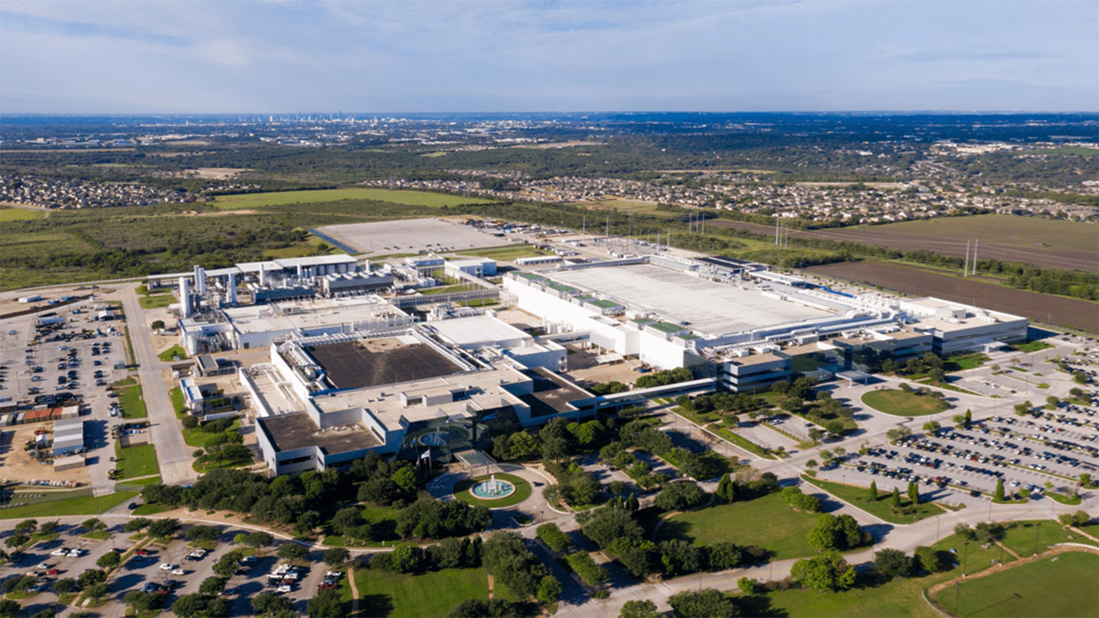
Samsung’s reported second semiconductor factory in Taylor, Texas, would put a critical part of advanced artificial-intelligence memory into US production but not the entire product, and not until 2030. The approximately 2.7-million-square-foot facility, known as Taylor Fab 2, is reportedly planned to manufacture high-bandwidth-memory base dies exclusively for AMD and Nvidia.
Construction was scheduled to begin in early November 2026, consistent with a company announcement that work on a second Taylor fab would start in November. The reported customer assignments, component scope and production date offer a more specific picture of what Samsung intends to build. At about 1.5 times the size of Taylor Fab 1, the new plant would be a substantial addition to the company’s Texas footprint, although its expected production start remains roughly four years away.
A US-made base for an international memory stack
High-bandwidth memory, or HBM, is assembled as a vertical stack rather than as a conventional set of memory chips placed separately on a board. Multiple DRAM core dies supply the memory capacity, while a logic component called the base die sits beneath them and manages communication between the memory stack and the AI processor.
That base die is the part Samsung reportedly intends to manufacture in Texas for AMD and Nvidia. The DRAM core dies would continue to be produced in South Korea before being combined with the Texas-made logic layer. The completed HBM device would therefore remain a transpacific product: a strategically important stage would move into US production, but the supply chain would not become fully domestic.
The split also illustrates why semiconductor localization is more complicated than opening a large fabrication building. An HBM stack depends on different die types, process technologies and assembly steps. Moving one sophisticated component can expand regional capacity and diversify where it is made, while leaving the final product dependent on materials and components crossing national borders.
Smaller process nodes raise the technical target
Current HBM4 base dies are made on a 4-nanometer process. Taylor Fab 2 reportedly targets 2-nanometer or more advanced manufacturing for its base dies. In practical terms, the plan places the Texas facility on the logic side of HBM production, where increasingly complex communication and control functions must fit beneath a dense stack of memory.
The node target is significant, but a planned process is not the same as qualified volume production. A new fab must progress through equipment installation, process qualification, factory qualification and customer-product qualification before it can deliver chips at scale. Samsung’s first Taylor factory provides the nearer-term measure of how effectively the company can complete that sequence in Texas.
Fab 1 remains under construction and is intended to support an approximately $16.5 billion supply agreement with Tesla for next-generation AI chips. It is expected to reach full operational capacity by the end of 2026 and then ramp toward production in 2027. Samsung has said tools are being installed and processes are entering qualification, making Fab 1’s execution relevant to the credibility of the more ambitious Fab 2 schedule.
The building is only one part of capacity
The scale of Fab 2 would also put pressure on the surrounding industrial system. Advanced fabs require reliable electricity, large volumes of water, specialized chemicals, equipment support and a trained workforce. A CSIS assessment of the Texas semiconductor ecosystem identifies dependable power and water, supplier coordination and workforce development as continuing constraints as the state adds fabrication capacity.
Samsung is already supporting workforce programs around Taylor, while the company’s first fab moves through startup and qualification. Those efforts matter because a 2.7-million-square-foot shell does not itself create usable chip output; the factory must be staffed, supplied, qualified and connected to the rest of the manufacturing chain.
If completed as reported, Fab 2 would give AMD and Nvidia a US source for an advanced HBM logic component and give Samsung a larger role in supplying AI-computing hardware. Its practical boundary is equally clear: the capacity would arrive in 2030, after Fab 1 has had several years to demonstrate Samsung’s Texas manufacturing execution, and every finished memory stack would still depend on DRAM dies arriving from South Korea.
| More aerospace and engineering stories, right in your MSN feed. Follow AMI on MSN |
By Thomas Caldwell — AMI’s senior editor for mechanical and mobility engineering, covering vehicle electronics, systems integration, electrification, chassis systems, propulsion, and safety policy.